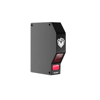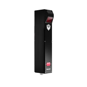
Gocator 2380 Product Parameters
|
Model |
Gocator 2380 |
|
Brand |
LMI |
|
Sensor type |
point laser sensor |
|
Data points |
1280 |
|
Field of View FOV (mm) |
390~1260 |
|
Measurement range MR (mm) |
800 |
|
Net distance (mm) |
350 |
|
X-direction resolution (µ m) |
375~1100 |
|
Z-direction resolution (µ m) |
92~488 |
|
Z-direction linearity (% of MR) |
0.04 |
|
Z-direction repeatability accuracy (µ m) |
12 |
|
Laser grade |
2,3R |
|
Scanning rate/time |
0.17 ~ 5 kHz |
|
Data interface |
GigE |
|
Power supply |
24 ~ 48 VDC,13W |
|
Protection level |
IP67 |
|
Dimensions |
49 mm × 75 mm × 272 mm(side mounted) |
|
Working temperature |
0℃ ~ +50℃ |
|
Weight |
1.3 kg |
Product feature of the Gocator 2380
- High-precision 3D scanning, precise measurement
1280 points/contour, megapixel resolution, accurate capture of micron-level details
5000 Hz high-speed scanning to meet the online detection needs of high-speed production lines
Monochrome laser brightness image, efficient detection of surface defects such as cracks, scratches, dents, etc.
- Intelligent operation, ready to use
Built-in measurement tools, no programming required, simplifying the detection process and improving detection efficiency
Direct setting and control by web browser, no additional software required, remote management supported
Low-latency data processing to ensure real-time and accurate measurement
- Efficient data communication, easy expansion
Gigabit Ethernet data transmission to ensure high-speed and stable data communication
Support multi-sensor online system, expand the detection range and improve measurement accuracy
- Industrial-grade design, adapt to harsh environments
IP67-level industrial protective housing, waterproof and dustproof, suitable for various complex industrial environments
Compact and lightweight design, easy to integrate into automated production equipment
Product application of the Gocator 2380
Semiconductor and Electronic Manufacturing Applications
- Wafer Defect Detection
Ultraviolet (UV) light is ideal for penetrating thin-layer materials such as photoresist, enabling the detection of sub-micron level surface defects and pattern distortions. This capability improves chip yield by identifying defects early in the production process.
- Microcircuit Quality Inspection
UV light is highly effective in inspecting PCB solder joints and detecting hidden cracks or contamination in microcircuits. By avoiding interference from visible light reflection, UV light ensures precise and accurate defect localization, enhancing overall circuit board quality.
- Packaging Material Analysis
UV light enhances the detection of inconsistencies in packaging materials, such as the uniformity of adhesive layers or the presence of bubbles. This light also improves imaging contrast, making it easier to identify defects in organic materials that absorb UV light at a higher rate, ensuring better quality control during packaging.
Dimensions

Installation and debugging support
Hardware installation guidance:
Guide customers to complete the installation of the camera, including mechanical fixation, line layout, interface connection, etc.
Software debugging:
- Provide installation support for camera drivers and software platforms.
- Assist in configuring parameters such as exposure, gain, frame rate, etc. to ensure the best effect of the camera in actual application.
- Interface with the customer's host computer software system to ensure smooth data acquisition and processing.
Hot Tags: gocator 2380, China gocator 2380 suppliers, MV-CU004-10GM, , MER3-1221-24G3C-P, MER2-280-139U3C-L, MV-CS200-10GC, MV-CE013-80UM