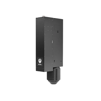
Gocator 4010 Product Parameters
|
Model |
Gocator 4010 |
|
Brand |
LMI |
|
Sensor type |
Confocal sensor |
|
Data points |
1920 |
|
Field of View FOV (mm) |
3.5 |
|
Measurement range MR (mm) |
1.05 |
|
Net distance (mm) |
9.3±0.2 |
|
X-direction resolution (µ m) |
1.9 |
|
Z-direction linearity (% of MR) |
0.06 |
|
Z-direction repeatability accuracy (µ m) |
0.12 |
|
Scanning rate/time |
4.3 ~ 14 kHz |
|
Maximum tilt angle (°) |
45 ~ 85 |
|
Data interface GigE |
GigE |
|
Power supply |
24 ~ 48 VDC,77W |
|
Protection level |
IP50 |
|
Mechanical dimensions |
82 mm × 183 mm × 459 mm |
|
Working temperature |
+15℃ ~ +35℃ |
|
Weight |
10.4 kg |
Product feature of the Gocator 4010
1. Ultra-High Precision & High-Speed Scanning
Generates 1,920 data points per scanned contour, capturing fine details with exceptional clarity.
Fast scanning rate, ensuring real-time 3D measurement and inspection.
X-direction resolution of 1.9 μm, enabling ultra-precise feature detection.
2. Advanced Coaxial Optical Design
Shadow-free scanning, ideal for complex geometries and challenging materials.
Maximum tilt angle of ±85°, providing excellent adaptability for curved and inclined surfaces.
Superior performance on highly reflective materials, ensuring accurate measurement on metals, glass, and polished surfaces.
3. Versatile & Intelligent Inspection Capabilities
Accurately scans any material or part shape, making it suitable for diverse manufacturing applications.
Built-in 3D measurement and inspection software, simplifying integration and operation.
Seamless compatibility with automated production lines, enhancing efficiency in smart manufacturing.
Product application of the Gocator 4010
1. Semiconductor and Electronic Manufacturing
- Wafer defect detection: Ultraviolet light can penetrate thin layer materials (such as photoresist), identify sub micron level surface defects or pattern distortions, and improve chip yield.
- Microcircuit detection: used for detecting the quality of PCB solder joints, hidden cracks or contamination of micro circuits. UV light can avoid visible light reflection interference and accurately locate defects.
- Packaging material analysis: detect the uniformity or bubbles of the packaging adhesive layer, and enhance the imaging contrast of organic materials with high absorption rate of ultraviolet light.
2. Materials Science and Coating Testing
- Fluorescent material analysis: Excitation of the fluorescent properties of composite materials or biological samples for chemical composition identification or pollutant identification (such as oil stains and residual chemicals).
- Coating thickness and uniformity: The penetration ability of ultraviolet light on coatings (such as UV curing adhesives) can be monitored in real-time to ensure thickness consistency during the coating process.
3. Precision machining and micro nano manufacturing
- UV laser processing monitoring: In conjunction with UV lasers (such as 355 nm wavelength), real-time observation of the heat affected zone or deformation during micro processing (etching, drilling).
- 3D printing tomography detection: utilizing the high resolution of ultraviolet light to detect the accuracy of printed structures layer by layer, avoiding interlayer misalignment or insufficient material curing.
Dimensions

Hot Tags: gocator 4010, China gocator 4010 suppliers, 13 MP industrial USB 3 0 Camera, MV-CA050-20GM, MARS-1610-52GTM, MV-CE013-80UM, 4k cameralink color line camera

