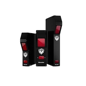
Gocator 1390 Product Parameters
|
Model |
Gocator 1390 |
|
Brand |
LMI |
|
Sensor type |
point laser sensor |
|
Measurement range MR (mm) |
2000 |
|
Net distance (mm) |
500 |
|
Z-direction resolution (µ m) |
25.0~60.0 |
|
Z-direction linearity (% of MR) |
0.1 |
|
Laser grade |
3B |
|
Scanning rate/time |
32 kHz |
|
Data interface |
GigE |
|
Power supply |
24 ~ 48 VDC,13W |
|
Protection level |
IP67 |
|
Mechanical dimensions |
330 mm × 120 mm × 277 mm(side mounted) |
|
Working temperature |
0℃ ~ +50℃ |
|
Weight |
1.25 kg |
Product feature of the Gocator 1390
- Ultra-high-speed scanning, precise measurement
32kHz ultra-high-speed scanning enables efficient dynamic measurement to meet the needs of high-precision online detection.
High-resolution measurement can accurately detect small size changes, with a measurement range of up to 2 meters, suitable for a variety of workpiece size requirements.
- Compact design, easy to integrate
Narrow body shape, optimized scanning density, can still provide fine measurement effects in a small space.
Modular architecture can be easily expanded to multi-sensor systems to achieve a wider range of 3D measurements.
- Efficient data transmission and system compatibility
Gigabit Ethernet is used to ensure high-speed data transmission and adapt to high-throughput industrial applications.
Rich I/O and PLC interfaces can be seamlessly integrated into various automation control systems to achieve intelligent measurement.
- Industrial-grade durability, adapt to complex environments
IP67-level protective housing, dustproof and waterproof, suitable for harsh industrial environments.
Class 3B laser level, providing stable high-precision measurement while taking into account industrial safety.
Product application of the Gocator 1390
Semiconductor and Electronic Manufacturing
- Wafer defect detection: Ultraviolet light can penetrate thin layer materials (such as photoresist), identify sub micron level surface defects or pattern distortions, and improve chip yield.
- Microcircuit detection: used for detecting the quality of PCB solder joints, hidden cracks or contamination of micro circuits. UV light can avoid visible light reflection interference and accurately locate defects.
- Packaging material analysis: detect the uniformity or bubbles of the packaging adhesive layer, and enhance the imaging contrast of organic materials with high absorption rate of ultraviolet light.
Precision machining and micro nano manufacturing
- UV laser processing monitoring: In conjunction with UV lasers (such as 355 nm wavelength), real-time observation of the heat affected zone or deformation during micro processing (etching, drilling).
- 3D printing tomography detection: utilizing the high resolution of ultraviolet light to detect the accuracy of printed structures layer by layer, avoiding interlayer misalignment or insufficient material curing.
Dimensions


Installation and debugging support
Hardware installation guidance:
Guide customers to complete the installation of the camera, including mechanical fixation, line layout, interface connection, etc.
Software debugging:
- Provide installation support for camera drivers and software platforms.
- Assist in configuring parameters such as exposure, gain, frame rate, etc. to ensure the best effect of the camera in actual application.
- Interface with the customer's host computer software system to ensure smooth data acquisition and processing.
Hot Tags: gocator 1390, China gocator 1390 suppliers, ME2S-1260-9GC-P, MV-CS200-10UM, 1 6MP industrial boardlevel camera, MARS-3140-3GC-P, MER2-2000-6GM-P